6.1.2. Interface LTC-6820 v1.0.3
6.1.2.1. Overview
Important
The following description only applies for the LTC LTC6820-based
BMS-Interface hardware version 1.0.3.
Hint
All connector pinouts described below follow the Convention for Molex Micro-Fit 3.0 Connector Pin Numbering and Convention for Samtec Edge Rate connectors.
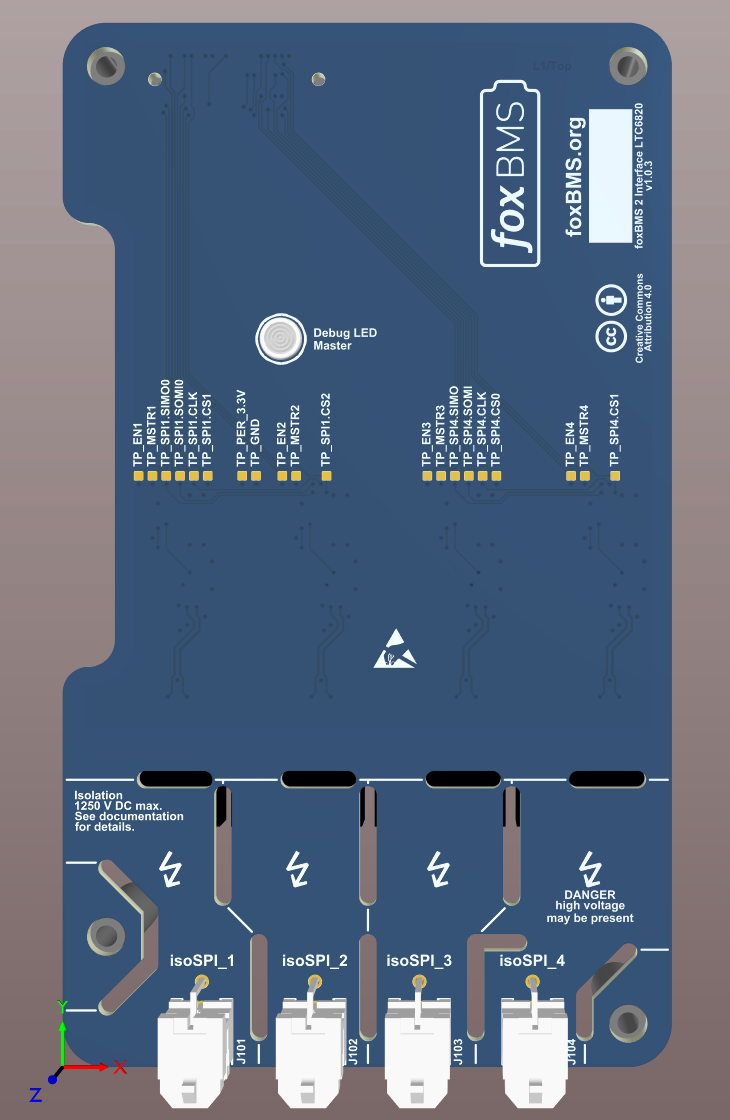
The BMS-Interface is used to enable communication between the BMS-Master and the BMS-Slaves. A 3D rendering of the BMS-Interface is shown in Fig. 6.1. The BMS-Interface is intended to be used together with a BMS-Master.

Fig. 6.1 3D rendering of the BMS-Interface
6.1.2.2. Specifications
6.1.2.2.1. Mechanical Dimensions
The size of the PCB is 70 mm x 120 mm. A 3D-model and a drawing of the PCB can be found in section Design Resources.
6.1.2.2.2. isoSPI Insulation
The interface board is designed for a maximum continuous insulation voltage of 1250 V DC between all four isoSPI channels and between each isoSPI channel and the BMS-Master.
The insulation is designed according to DIN EN 60664-1:2008-01 under the following conditions:
Type of insulation: functional
Electrical field: homogeneous
Pollution degree: 2
PCB insulator class: 3b
Transient voltage: 4300 V DC
Continuous (working) voltage: 1250 V DC (selected due to design space constraints on PCB)
The PCB design complies with the following parameters:
Clearance: 1.3 mm
Creepage distance: 12.5 mm
6.1.2.2.3. Block Diagram
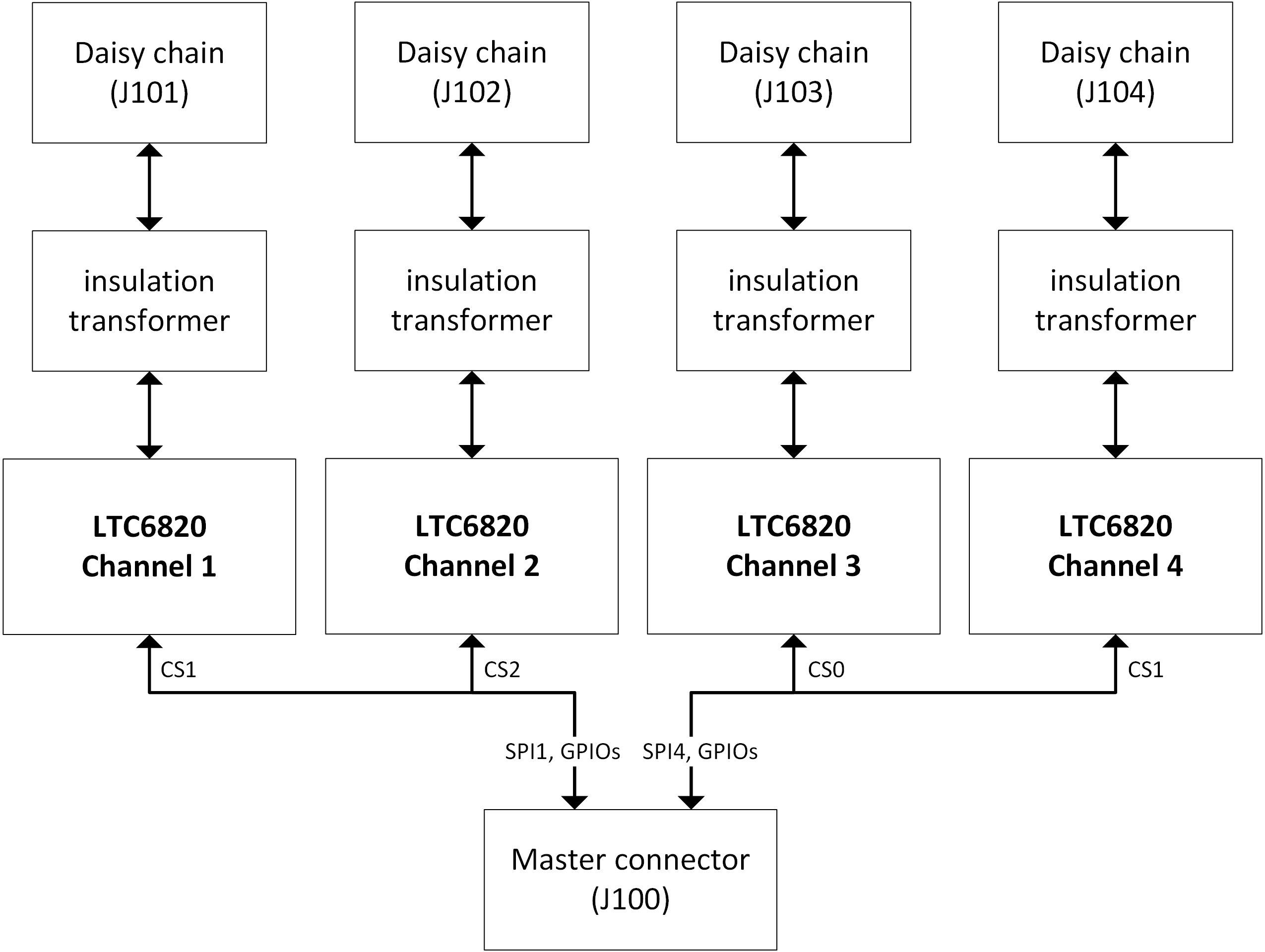
A block diagram of the BMS-Interface is shown in Fig. 6.2.

Fig. 6.2 Block diagram of the BMS-Interface
Each of the four isoSPI channels uses one LTC LTC6820 communication chip from Analog Devices and an insulation transformer. The LTC LTC6820 chips are directly connected to the MCU via SPI.
6.1.2.2.4. Schematic and Board Layout
More information about the board schematic and layout files can be found in section Design Resources. For better debugging, there are test-points on the PCB for all relevant IO signals.
6.1.2.3. Functions
6.1.2.3.1. isoSPI communication
The BMS-Interface offers up to four isolated isoSPI communication channels using the LTC LTC6820 transceiver chip from Analog Devices. The LTC LTC6820 transceivers are controlled by the SPI signals from the BMS-Master. The isoSPI signals are available on the connectors J101, J102, J103 and J104. The pinout of these connectors is described in Table 6.1.
Pin |
Signal |
Description |
|---|---|---|
1 |
|
isoSPI positive |
2 |
|
isoSPI negative |
For the connection to the BMS-Master, a 40-pole mezzanine connector (J100) is used. The pinout and pin usage is described in Table 6.2.
Pin |
Signal |
Description |
Usage on BMS-Interface |
|---|---|---|---|
1 |
|
- |
isoSPI channel 1/2 |
2 |
|
- |
- |
3 |
|
- |
isoSPI channel 1/2 |
4 |
|
- |
- |
5 |
|
- |
isoSPI channel 1/2 |
6 |
|
- |
isoSPI channel 1 |
7 |
|
- |
isoSPI channel 2 |
8 |
|
- |
- |
9 |
|
- |
- |
10 |
|
- |
- |
11 |
|
- |
isoSPI channel 3/4 |
12 |
|
- |
isoSPI channel 3/4 |
13 |
|
- |
isoSPI channel 3/4 |
14 |
|
- |
isoSPI channel 3 |
15 |
|
- |
isoSPI channel 4 |
16 |
|
- |
- |
17 |
|
- |
- |
18 |
|
- |
- |
19 |
|
- |
- |
20 |
|
Interrupt pin, connected to MCU GIOA_2 |
- |
21 |
|
Interrupt pin, connected to MCU GIOA_3 |
- |
22 |
|
Interrupt pin, connected to MCU GIOA_4 |
- |
23 |
|
Interrupt pin, connected to MCU GIOA_6 |
- |
24 |
|
GPIO pin, connected to port expander 3 IO1_0 |
isoSPI channel 1 LTC LTC6820 enable |
25 |
|
GPIO pin, connected to port expander 3 IO1_1 |
isoSPI channel 1 LTC LTC6820 master |
26 |
|
GPIO pin, connected to port expander 3 IO1_2 |
isoSPI channel 2 LTC LTC6820 enable |
27 |
|
GPIO pin, connected to port expander 3 IO1_3 |
isoSPI channel 2 LTC LTC6820 master |
28 |
|
GPIO pin, connected to port expander 3 IO1_4 |
isoSPI channel 3 LTC LTC6820 enable |
29 |
|
GPIO pin, connected to port expander 3 IO1_5 |
isoSPI channel 3 LTC LTC6820 master |
30 |
|
GPIO pin, connected to port expander 3 IO1_6 |
isoSPI channel 4 LTC LTC6820 enable |
31 |
|
GPIO pin, connected to port expander 3 IO1_7 |
isoSPI channel 4 LTC LTC6820 master |
32 |
|
Power supply ground |
Power supply ground |
33 |
|
Power supply ground |
Power supply ground |
34 |
|
3.3 V from peripheral SBC |
3.3 V power supply |
35 |
|
3.3 V from peripheral SBC |
3.3 V power supply |
36 |
|
5.0 V from peripheral SBC |
- |
37 |
|
5.0 V from peripheral SBC |
- |
38 |
|
12 V from buck-boost converter |
- |
39 |
|
Master supply voltage (after protection circuits) |
- |
40 |
|
Master supply voltage (after protection circuits) |
- |
